Single-Layer Circuit Board

Single-Layer Circuit Board


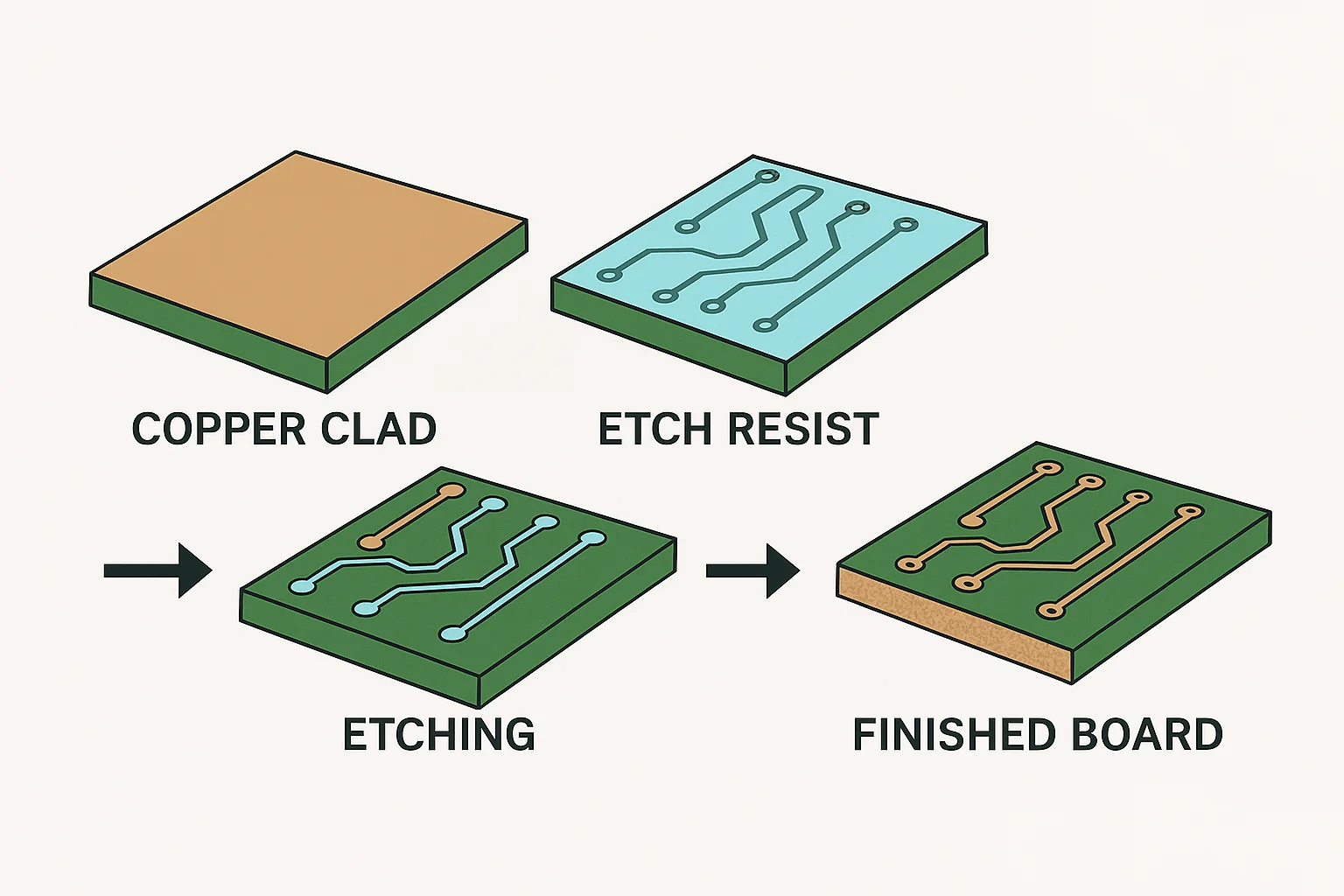
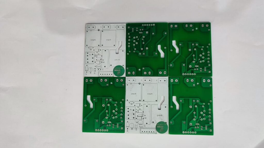
A Single Copper Layer Board, also known as a single-sided PCB, is the most fundamental type of printed circuit board. It consists of one conductive copper layer on one side of the board, while the opposite side is reserved for mounting components. This type of PCB is widely used in simple electronic devices due to its cost-effectiveness and ease of manufacturing. At Ittefaq Electrotech, we specialize in producing high-quality single copper layer boards tailored for reliable performance in everyday electronic applications.


Ideal Choice for Basic Electronic Applications

For simple and entry-level electronics, single-layer PCBs offer just the right balance of performance, ease of manufacturing, and affordability. They are commonly used in the following applications:

  • LED Lighting Systems
  • Calculators
  • Power Supplies
  • Consumer Electronics
  • Printers and Scanners
  • Kitchen Appliances
  • Audio Equipment
1

Copper Thickness

We offer copper layers ranging from 1 oz to 3 oz, allowing flexibility for various current and thermal requirements. This ensures durability and optimal conductivity in all designs.

2

Board Thickness

Our boards are available in thicknesses from 0.6mm to 2.0mm, providing options for lightweight electronics as well as more robust applications.

3

Minimum Hole Size

With precision drilling capabilities, we support hole sizes as small as 0.3mm, enabling compact layouts and reliable component fitting.

4

Surface Finish Options

We provide multiple surface finishes such as HASL (Lead-Free or Leaded), ENIG, and OSP to meet different soldering and performance needs while enhancing shelf life and reliability.

Why Ittefaq Electrotech is the Best Choice for PCB Services

Why Us for Single-Layer Circuit Board Production

High-Quality Manufacturing

We use advanced equipment and technology to ensure precise manufacturing of single-layer PCBs, meeting the highest industry standards.

Quality Assurance

Each PCB undergoes thorough quality checks, including electrical testing and visual inspections, to guarantee reliability and functionality.

Timely Production

We prioritize timely production, ensuring your single-layer PCBs are delivered within the agreed-upon timeline without compromising quality.

Competitive Pricing

Our efficient production process helps minimize costs, providing high-quality PCBs at competitive prices, without sacrificing performance.

Single-Layer Circuit Board Production

The Single-Layer Circuit Board Process involves the following key steps to create a functional and reliable PCB:

Design the PCB Layout

During the first step of manufacturing a single-layer Circuit Board, we start by using PCB design software like Eagle, KiCAD, or Altium. Then, we proceed by creating the circuit schematic and converting it into a PCB layout. Finally, we export the design in Gerber format.

Prepare Copper Board

We use high-quality materials, such as clean copper-clad laminate (FR4 or similar). The next step involves cutting the laminate to the required size. Afterward, we clean the copper surface using sandpaper or alcohol to remove any oxidation and ensure optimal adhesion for the subsequent layers.

Transfer PCB Layout

The PCB layout transfer involves printing the design onto a transparent sheet (for UV method) or glossy paper (for toner transfer), then aligning and transferring the layout onto the copper board using UV light or a hot iron.

Etching

The main process involves submerging the board in an etching solution (usually ferric chloride), which removes the unwanted copper, leaving only the desired traces. Finally, rinse the board thoroughly with water after etching.

Drill the Holes

Drill mounting and via holes where component leads will be inserted using a PCB mini drill or CNC machine for precision.

Clean and Inspect

An important step we truly focus on is removing the etch-resistant layer using acetone or alcohol. Afterward, we clean and inspect the board for any short circuits or broken tracks.

Solder Mask

Next, we apply a solder mask to protect the copper traces and prevent shorts. If using a UV solder mask, the board is cured under UV light to harden the mask, ensuring durability and reliability.

Quality Check and Testing

Quality Check and Testing involve inspecting the PCB for defects, performing electrical tests, and verifying functionality to ensure it meets design specifications and is reliable for use.

Get in Touch

Contact Us Today

If you have any questions about PCB manufacturing or would like to learn more about our fabrication services, feel free to contact our team. Our experts are ready to assist you with tailored solutions and guide you through every stage of your PCB project.

Scroll to Top