Here’s a clear, step-by-step explanation of how a PCB goes from concept to a finished product.
1. PCB Design and Schematic Creation
The process begins with an engineer creating a schematic diagram. This shows how all the electronic components connect to each other.
Once the schematic is ready, it’s converted into a PCB layout using design software. The layout defines:
Board dimensions
Component placement
Copper trace routing
Layer structure
When the design is finalized, Gerber files are generated—these files guide the manufacturer at every step.
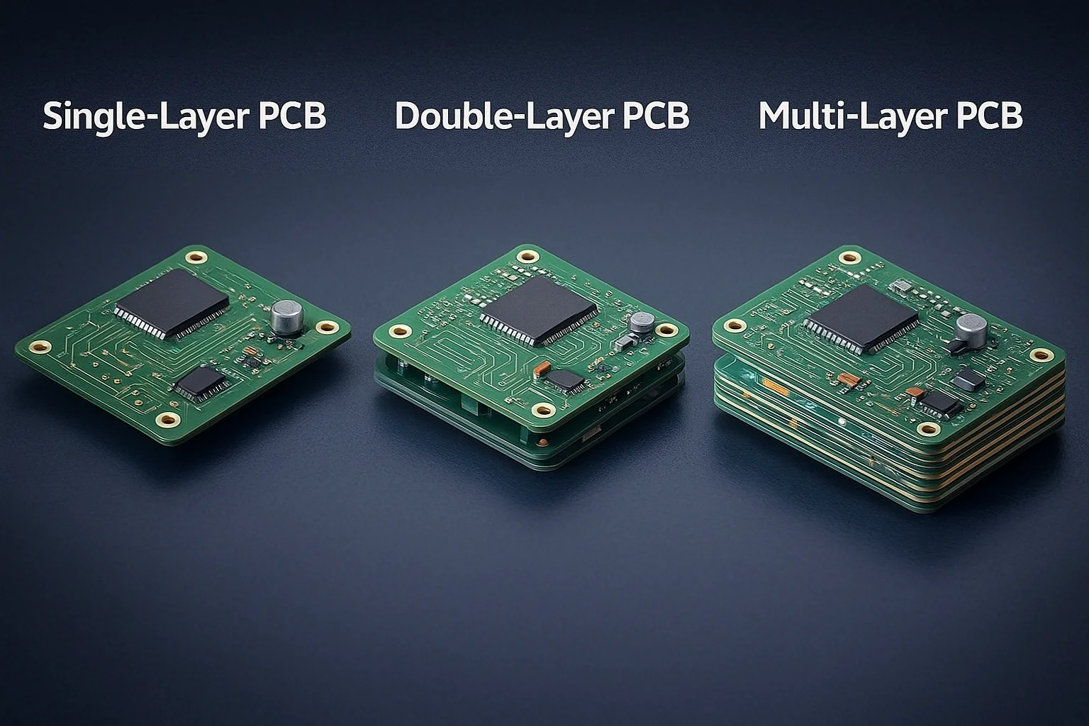
2. Material Selection
The base material, usually FR-4, provides strength, insulation, and heat resistance. Depending on the complexity, the PCB may be:
Single-layer
Double-layer
Multi-layer
Copper thickness and layer count are also decided at this stage.
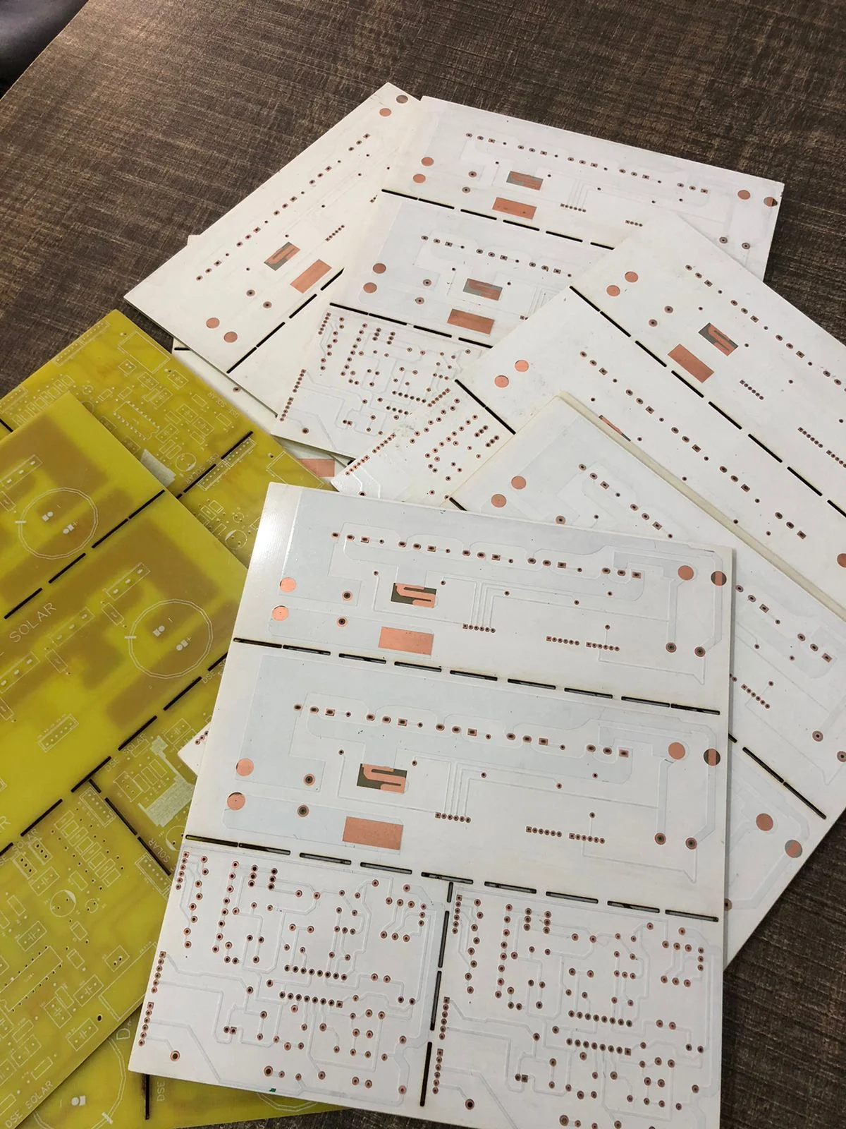
3. Printing the Circuit Pattern
The manufacturer transfers the PCB design onto the copper-clad board.
This is done using a photo-sensitive method, ensuring that the copper pattern matches the digital layout with high precision.
4. Etching the Copper
Next, unwanted copper is removed through an etching solution.
Only the copper that forms the circuit remains on the board.
This step defines the electrical pathways that carry signals and power.
5. Drilling Holes
Tiny holes are drilled for:
Component leads
Vias connecting different layers
Mounting points
Computer-controlled drilling machines ensure accuracy down to micrometers.
6. Plating and Layer Connection
For multi-layer and double-layer boards, the drilled holes are plated with copper.
This creates strong electrical connections between layers and ensures signal continuity across the board.
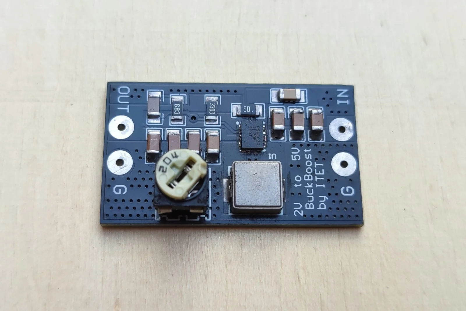
7. Applying the Solder Mask
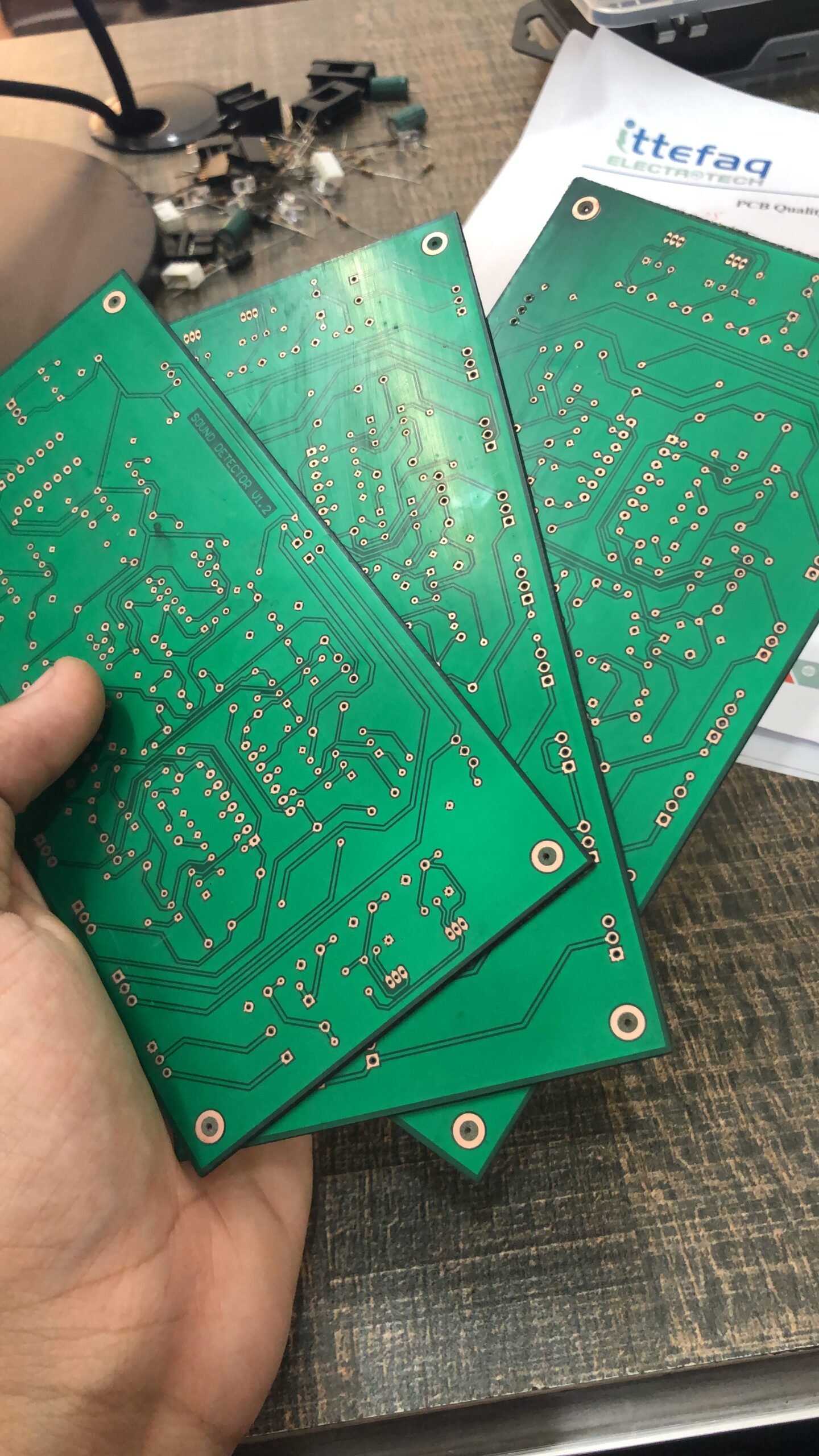
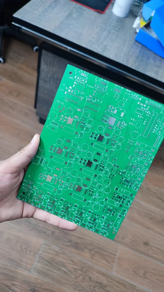
The familiar green coating you see on most PCBs is the solder mask.
It protects copper traces, prevents accidental short circuits, and ensures clean soldering during assembly.
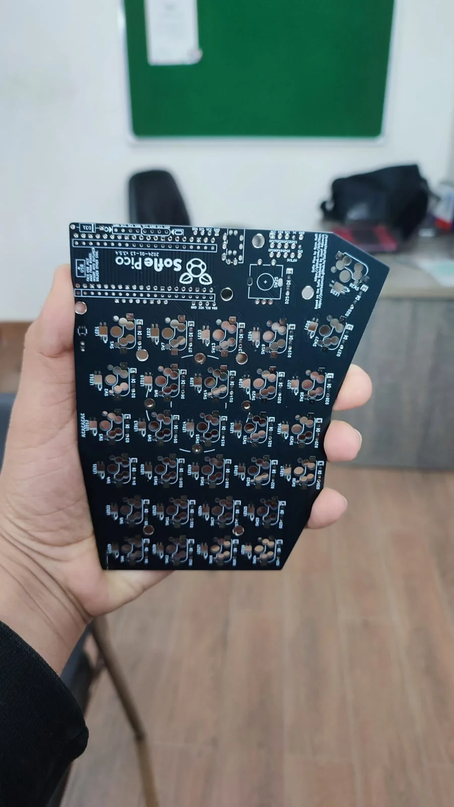
8. Silkscreen Printing
Labels, component markings, company logos, and test points are printed on the board.
This helps technicians assemble and troubleshoot the PCB later.
9. Surface Finishing
To prevent oxidation and improve solderability, a surface finish is applied to exposed pads.
Common finishes include:
HASL
ENIG (gold finish)
OSP
Immersion tin or silver
Each finish has different benefits depending on the device requirements.
10. Inspection and Testing
Before the board is approved, it goes through strict quality checks such as:
Visual inspection
AOI (Automated Optical Inspection)
Electrical continuity testing
This ensures the PCB matches the design and performs exactly as intended.
11. Final Cutting and Packaging
The finished PCB is cut into its final shape, cleaned, and packaged safely for delivery—ready for assembly into an electronic product.
Conclusion
From designing the circuit to applying finishes and testing, PCB manufacturing is a precise process that blends engineering, technology, and craftsmanship. Understanding these steps helps you appreciate the care and expertise behind every board.