What Is a PCB?
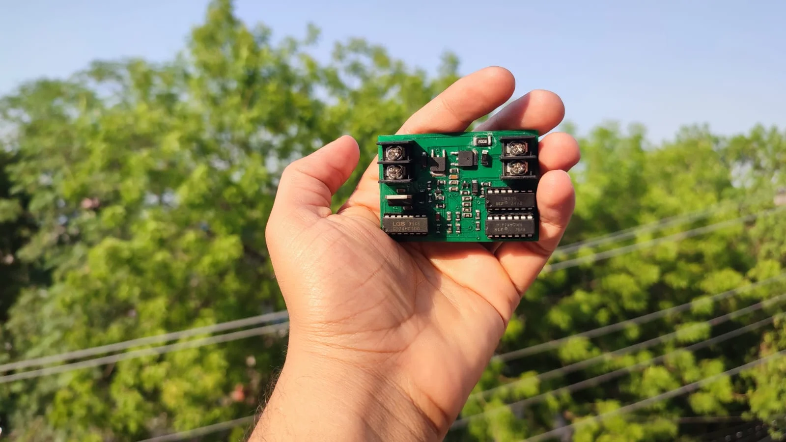
A PCB is a board that mechanically supports and electrically connects electronic components.
Instead of using loose wires, a PCB uses copper tracks, pads, and layers to form precise circuits that transfer signals and power.
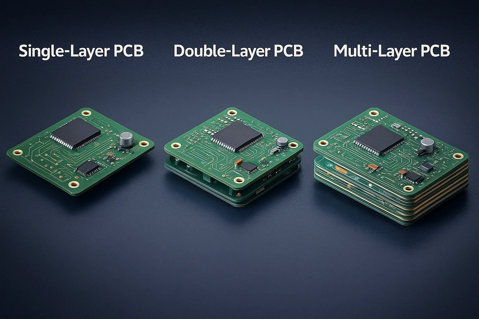
PCBs come in many types—single-layer, double-layer, and multi-layer—depending on how complex the circuit needs to be.
Why PCBs Are Important
PCBs are essential because they:
Keep circuits organized and compact
Improve the reliability of electronic devices
Ensure consistent performance
Allow products to be mass-produced with accuracy
Simply put, without PCBs, the modern electronics industry would not exist.
The PCB Manufacturing Process (Step by Step)
While the process can get technical, here’s a straightforward breakdown of how a typical PCB is made:
1. Designing the PCB
Every PCB starts as a design on specialized software (like Altium, Eagle, or KiCad).
The designer creates:
Component placement
Electrical connections (called “routing”)
Board shape and layer count
Safety clearances and spacing
A manufacturing-ready file called Gerber files is then generated.
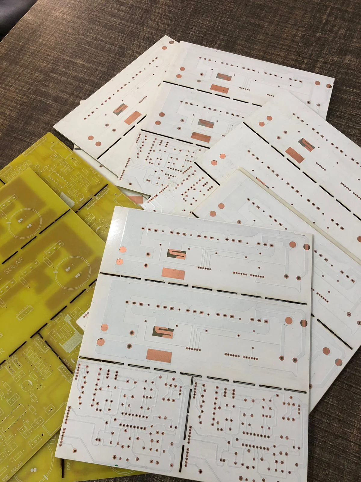
2. Selecting the Raw Material
The base of a PCB is normally FR-4, a fiberglass material known for strength and heat resistance.
This base is laminated with copper on one or both sides.
3. Transferring the Design to the Copper Board
The PCB pattern is printed or transferred onto the copper-clad board using a photographic process.
Wherever the pattern is applied, copper will stay.
Wherever it isn’t, the copper will later be removed.
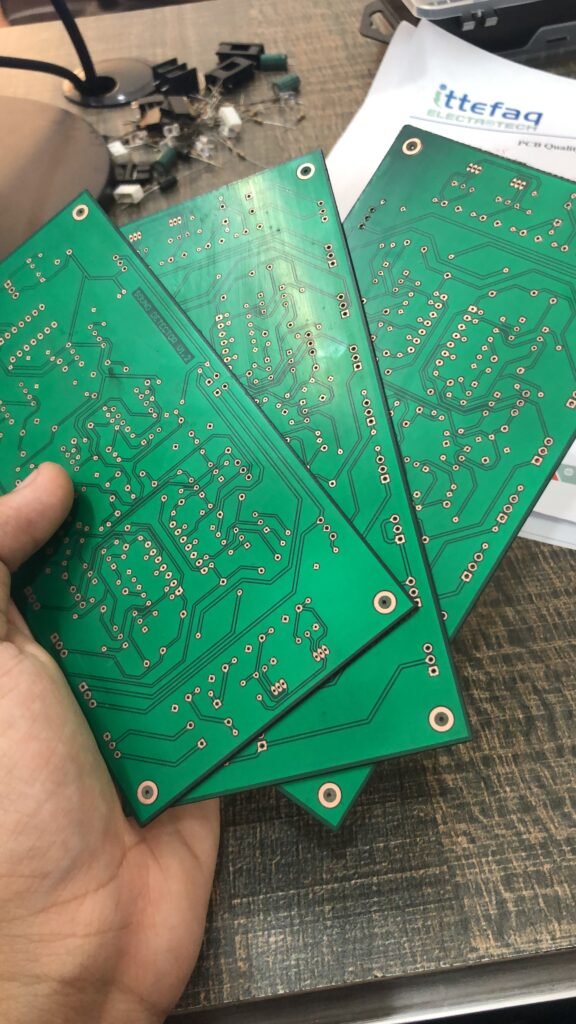
4. Etching – Creating the Copper Traces
Next, the board goes through an etching solution that removes unwanted copper.
This leaves behind clean copper tracks that match the PCB design.
This is one of the most important steps because these tracks act as the “wiring” of the circuit.
5. Drilling Holes for Components
Tiny holes are drilled with high-speed machines for:
Component leads
Vias (connections between layers)
Mounting holes
These drills must be extremely accurate—often controlled by computer-guided equipment.
6. Plating and Copper Deposition
For multi-layer and double-layer boards, the drilled holes need to conduct electricity.
A thin layer of copper is deposited inside each hole, creating solid connections between layers.
7. Applying the Solder Mask
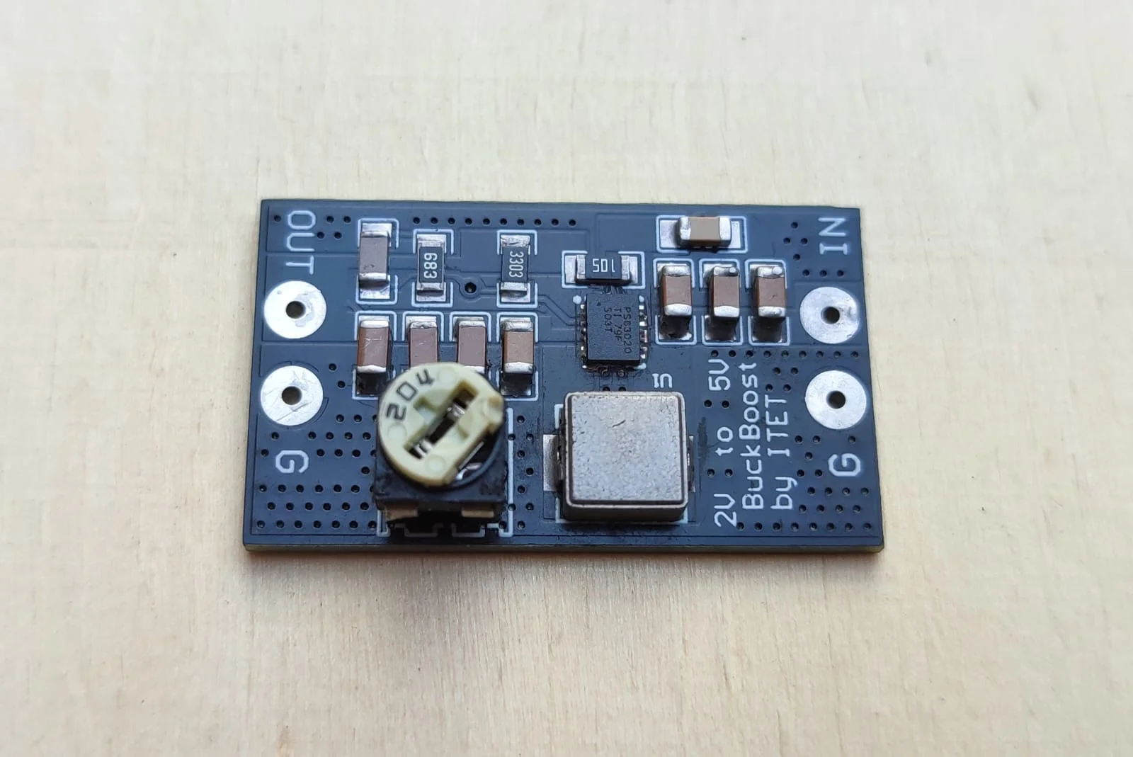
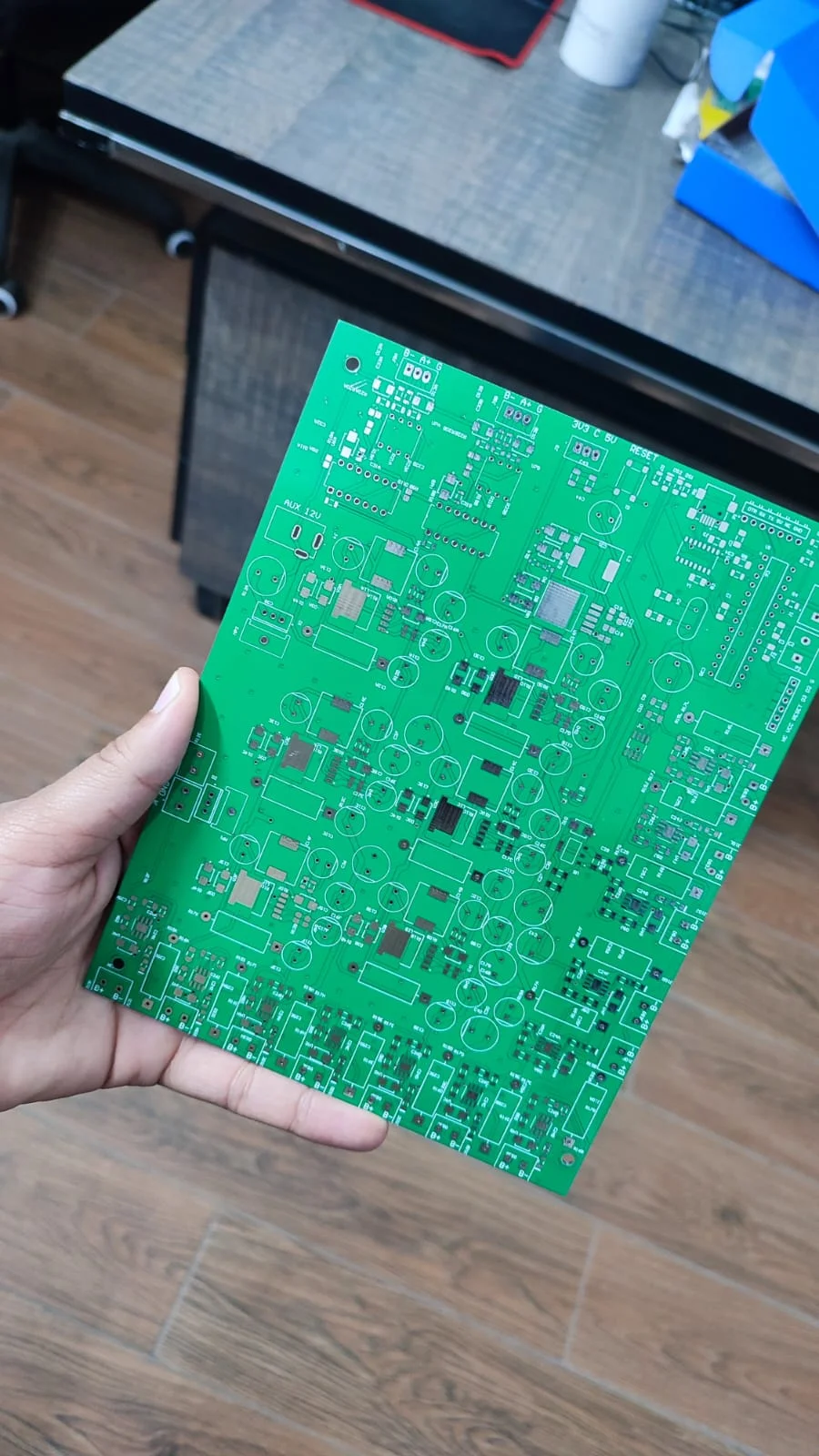
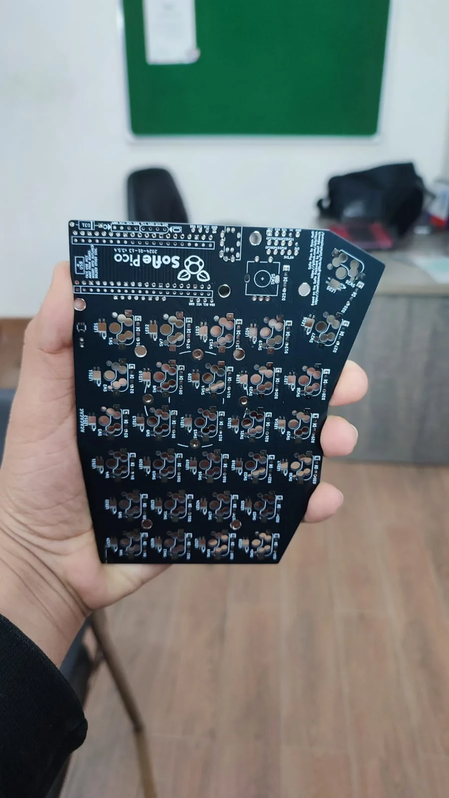
The green (or sometimes red, blue, or black) coating on a PCB is called the solder mask.
It protects the copper traces and stops solder from spreading during assembly.
This layer also gives the PCB its characteristic appearance.
8. Adding Silkscreen Text
The white text you see on a PCB—component labels, logos, numbers—is the silkscreen layer.
It helps during assembly and future repairs.
9. Surface Finishing
To protect exposed copper pads from oxidation and to make soldering easier, a surface finish is applied.
Common finishes include:
HASL (Hot Air Solder Leveling)
ENIG (Electroless Nickel Immersion Gold)
OSP (Organic Solderability Preservative)
Each option has different benefits depending on the product.
10. Final Inspection and Testing
Before delivery, each board is carefully checked.
Manufacturers use:
Electrical testing
Visual inspection
Automated optical inspection (AOI)
The goal is to ensure the board matches the design and works perfectly.
Where PCBs Are Used
PCBs power thousands of applications, such as:
Consumer electronics (phones, TVs, laptops)
Industrial machines
Security systems
Automotive electronics
Medical devices
IoT gadgets
Renewable energy equipment
Anywhere you find electronics, you’ll find PCBs.
Why Choosing the Right PCB Manufacturer Matters
A well-made PCB improves performance, reliability, and lifespan of your device.
A poorly made PCB can lead to overheating, short circuits, or complete device failure.
A reliable manufacturer ensures:
Accurate copper thickness
Proper material selection
Smooth edges and drilling
Clean solder mask application
Strict quality control
This is where companies like Ittefaq Electrotech stand out—combining precision, experience, and advanced processes to create boards that perform consistently in real-world conditions.
Final Thoughts
PCB manufacturing may look complex, but it follows a clear and logical process.
From design to drilling to finishing, each step plays a vital role in creating a board that brings your electronic ideas to life.
Whether you’re working on a prototype or preparing for mass production, understanding the basics helps you make better decisions and build better products.