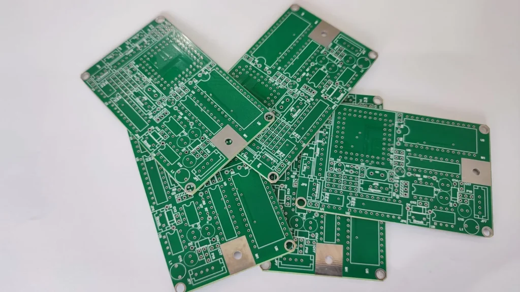
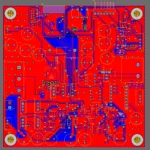


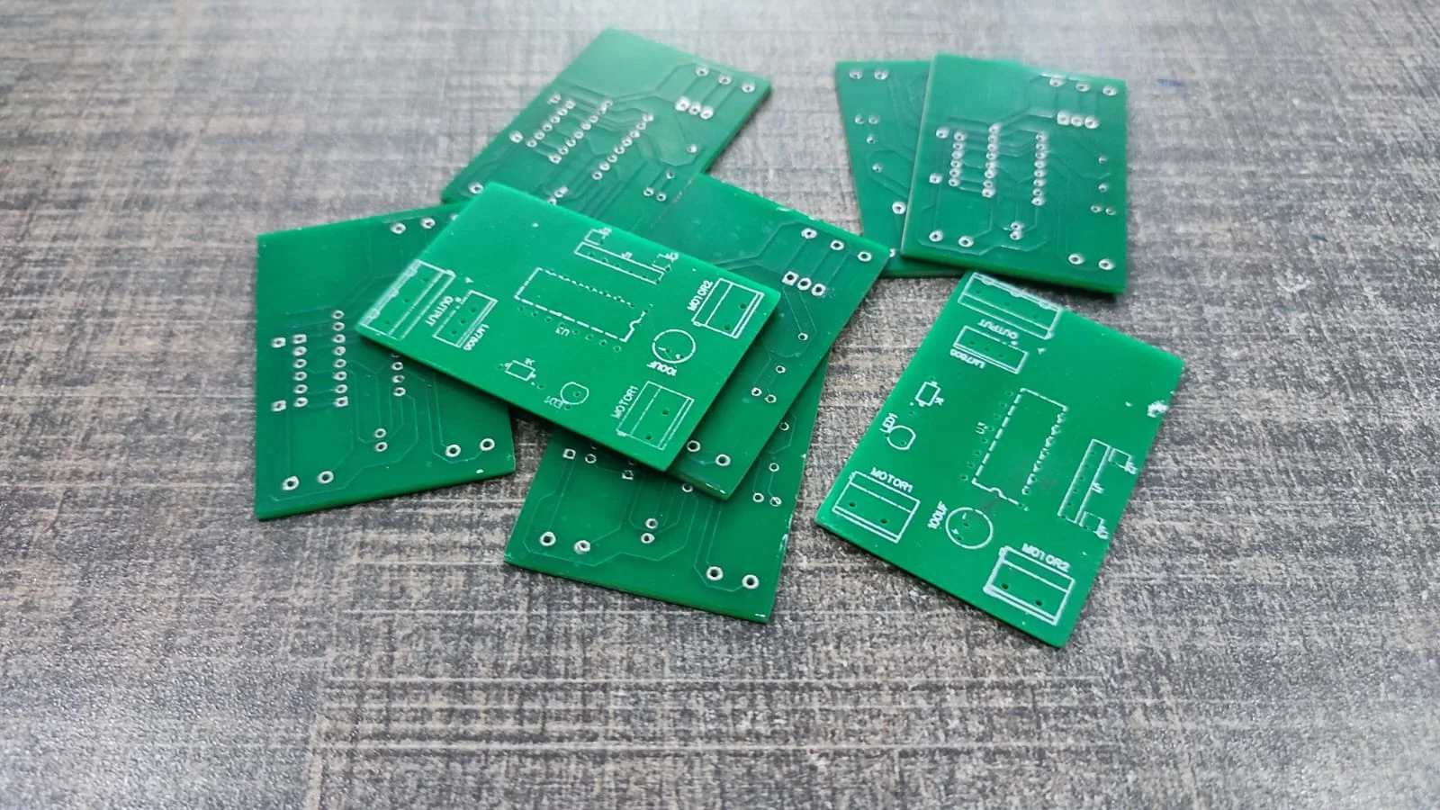
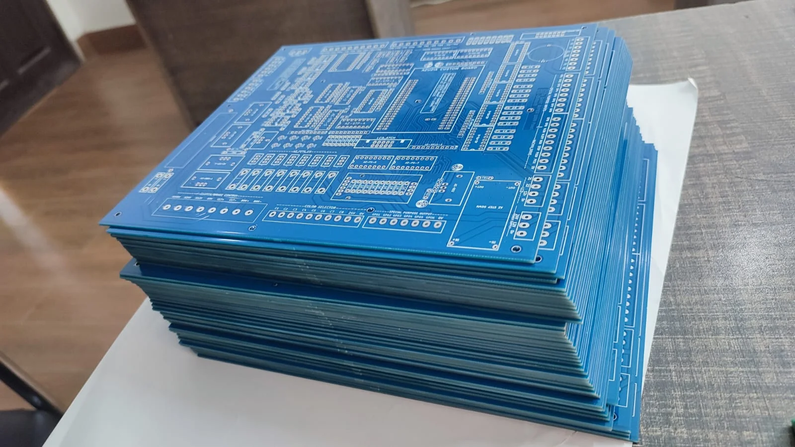
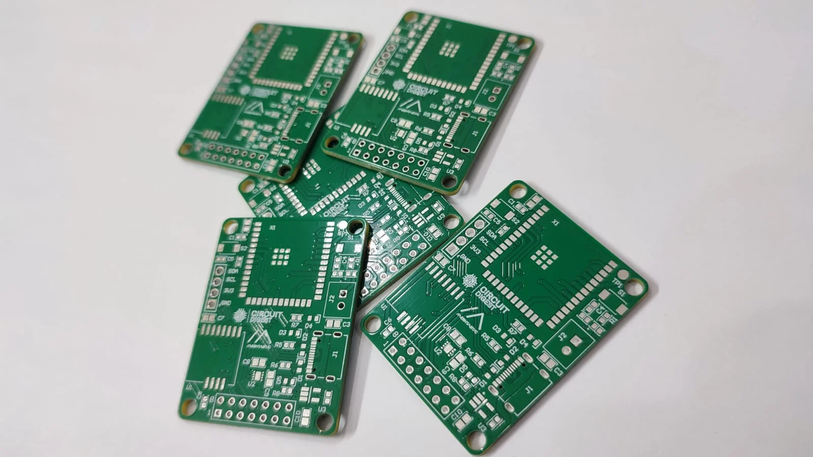
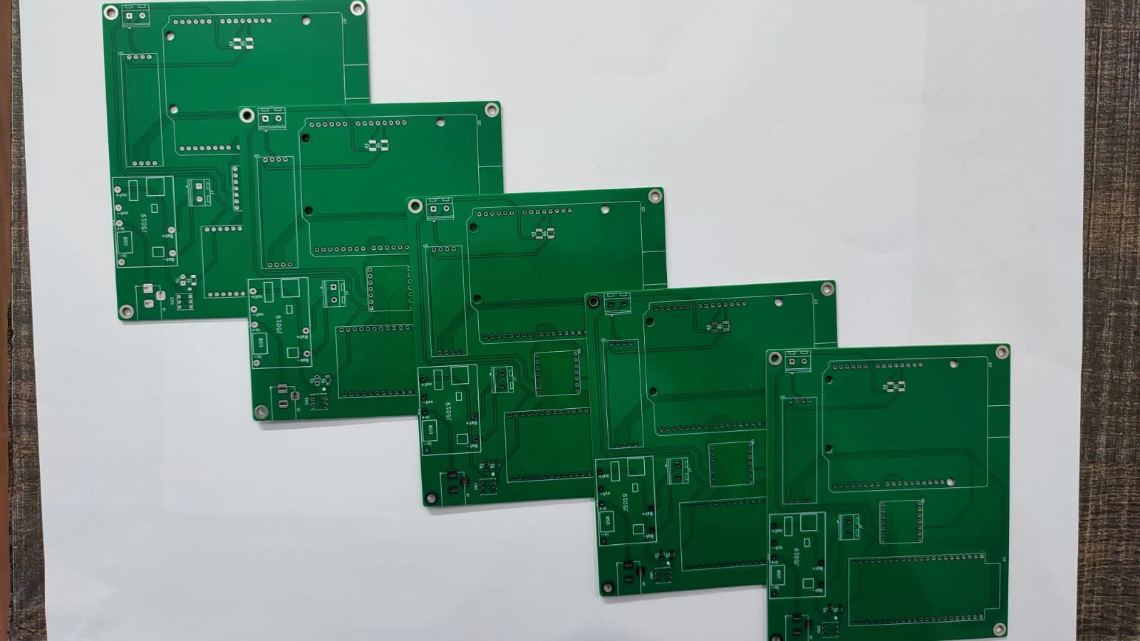
Printed Circuit Boards (PCBs) are the essential foundation for almost every modern electronic device. From smartphones to automotive systems, medical devices to consumer electronics, PCBs ensure the functionality of devices by providing both mechanical support and electrical connectivity for their components.
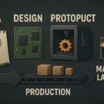
PCB manufacturing refers to the process of creating PCBs, which are the key components that connect and support the various electrical elements of electronic devices. The process includes several stages, such as design, material selection, prototyping, assembly, and testing, to ensure the PCB performs accurately and reliably.
Design and Prototyping
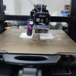
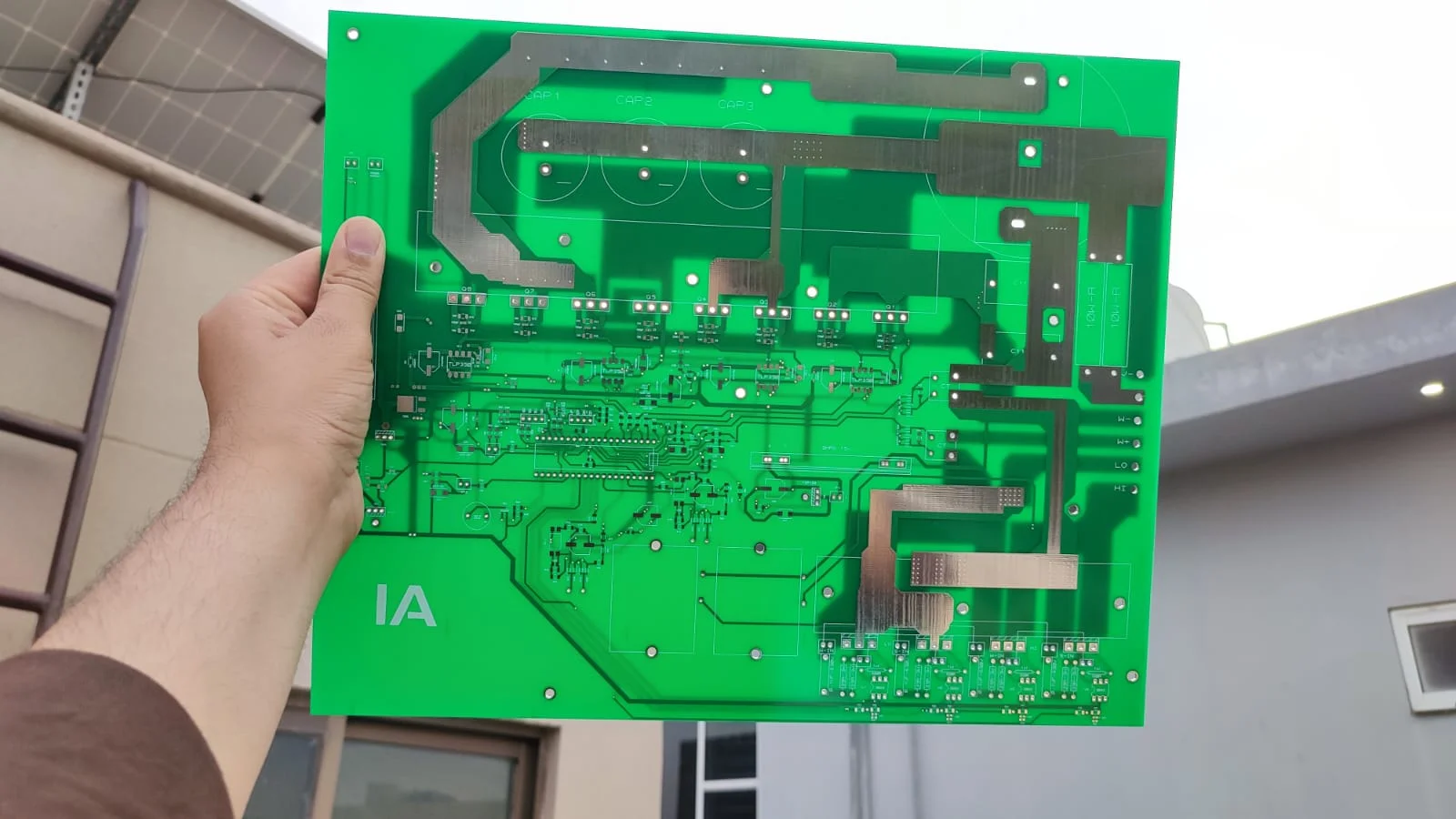
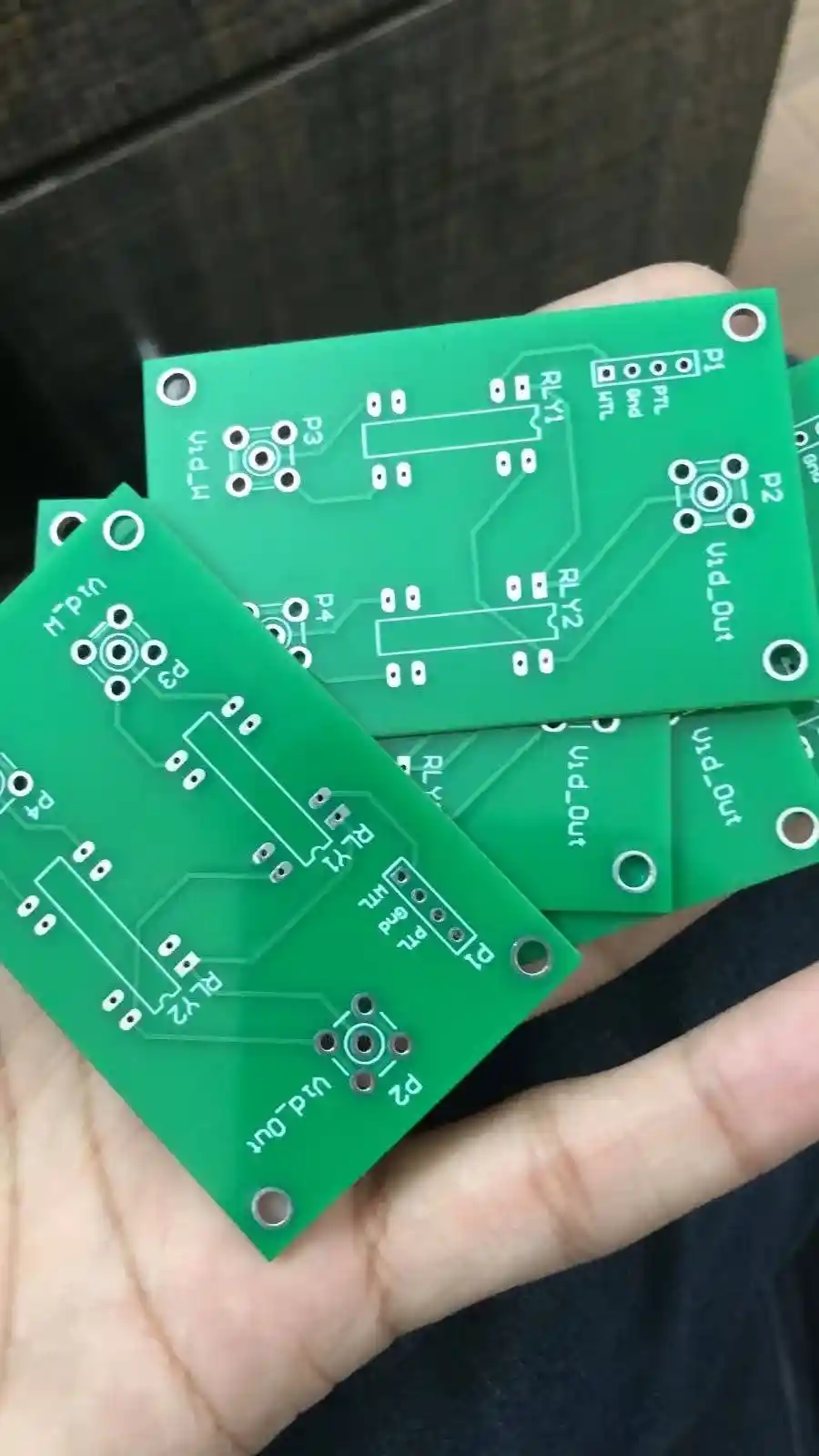
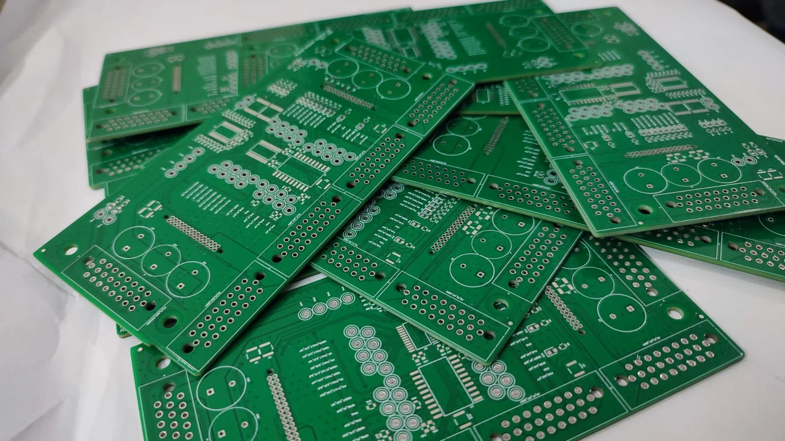
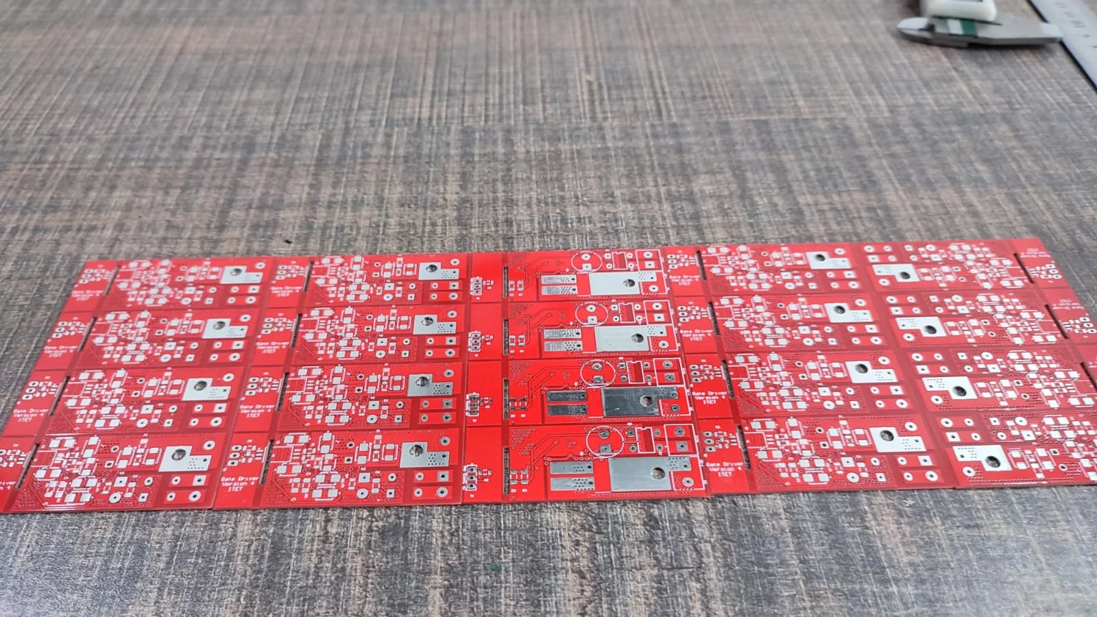
The first step in PCB manufacturing is design. Engineers create a layout of the PCB, detailing the connections between components. This design is often done using PCB design software. Once the design is finalized, a prototype is created to test the layout and functionality.
Material Selection
Choosing the right materials for the PCB is crucial. Common materials include fiberglass (FR4), flexible polymers, and ceramics, which provide varying levels of durability, conductivity, and flexibility.
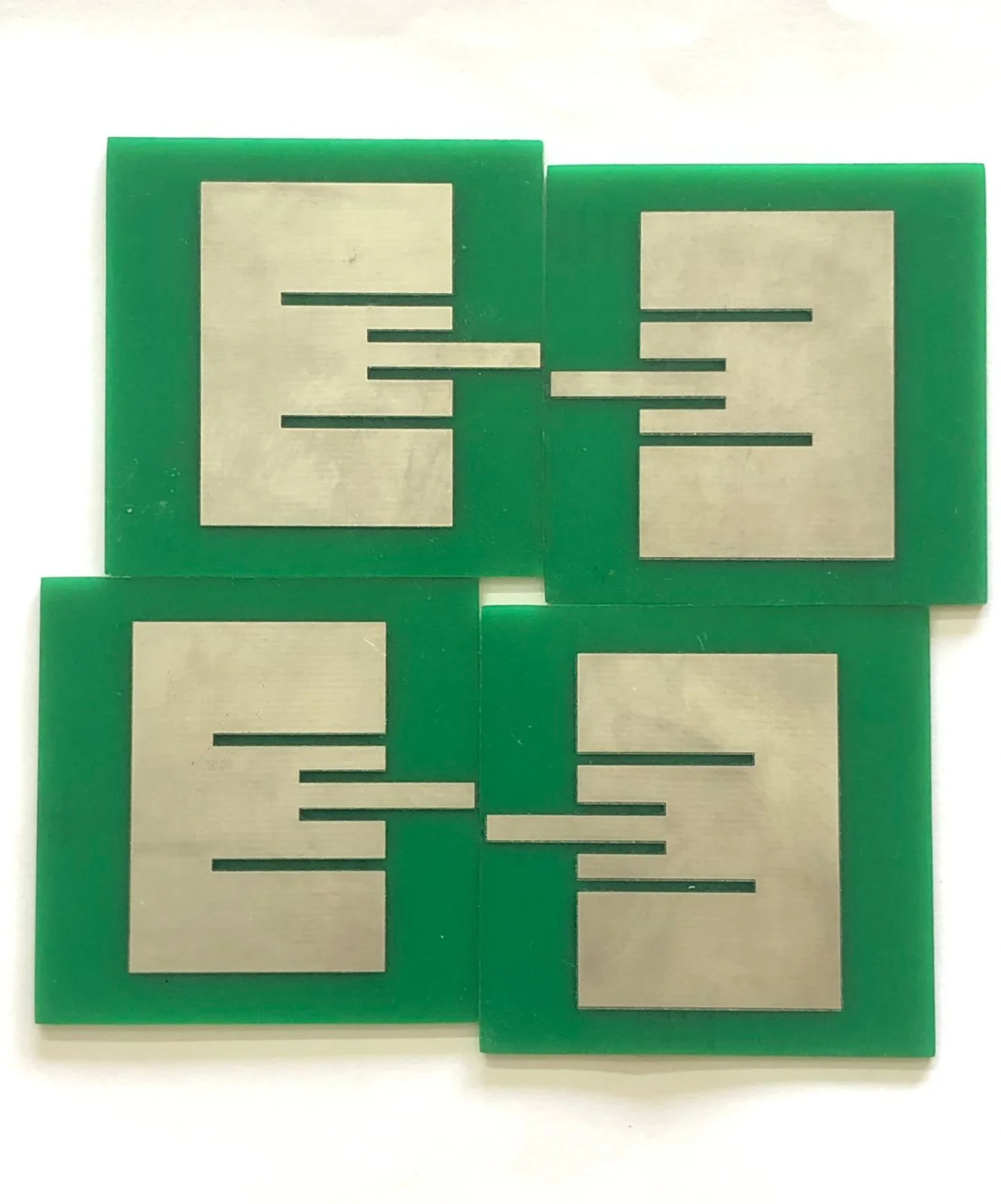
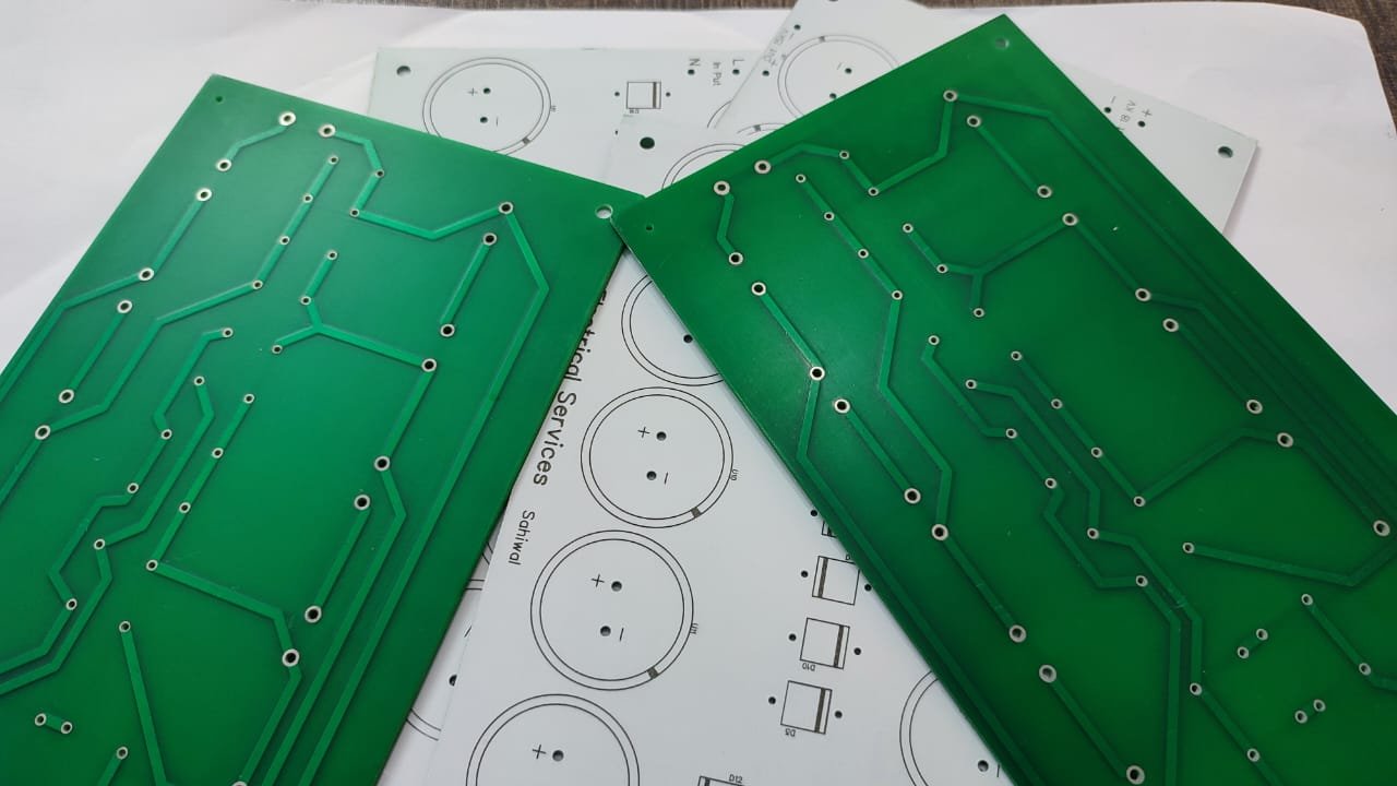
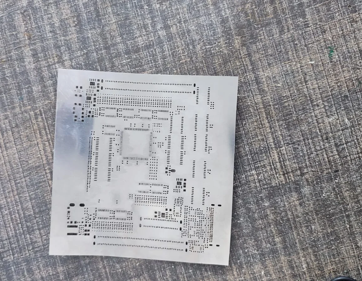
Printing and Etching
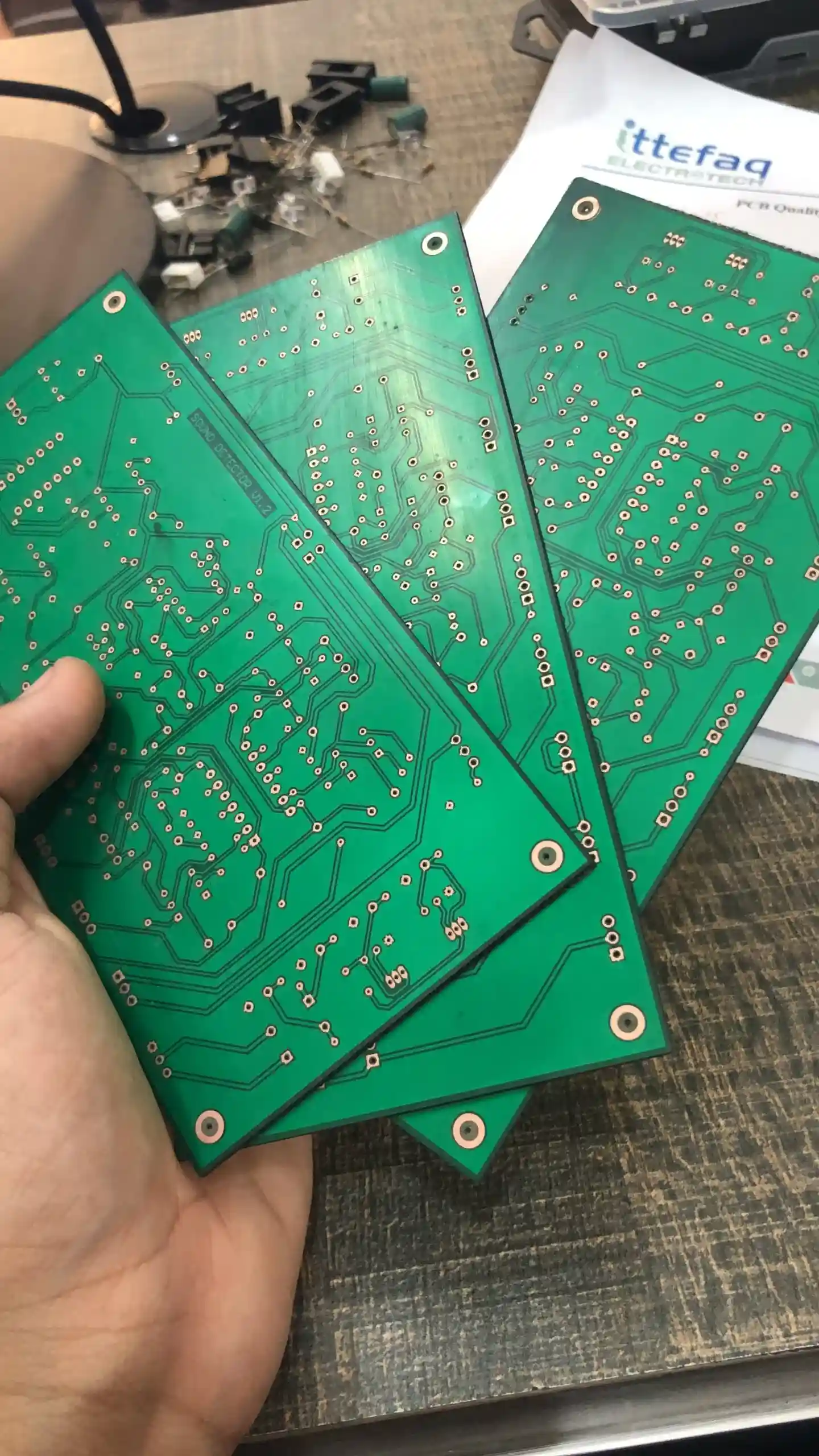
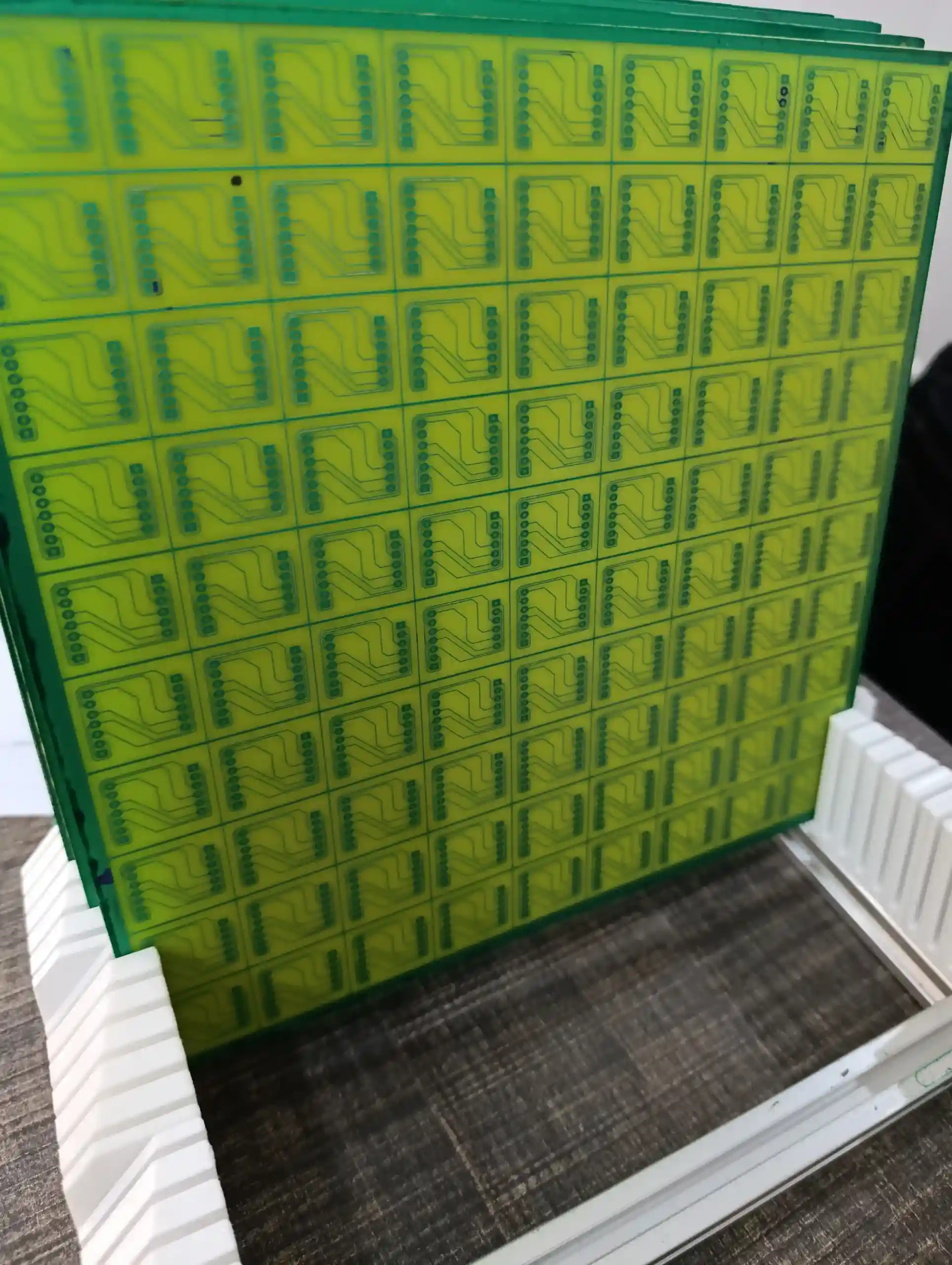
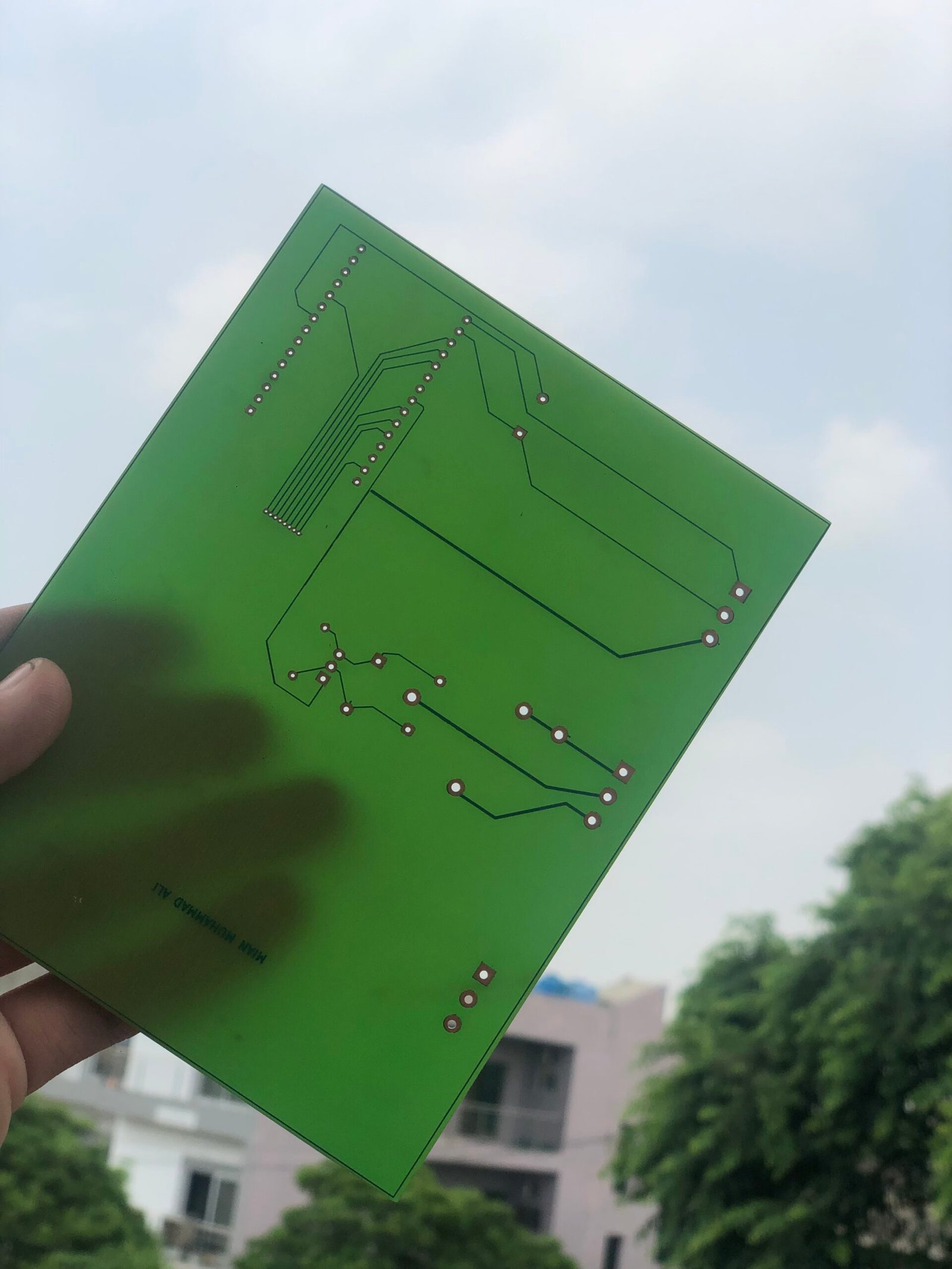
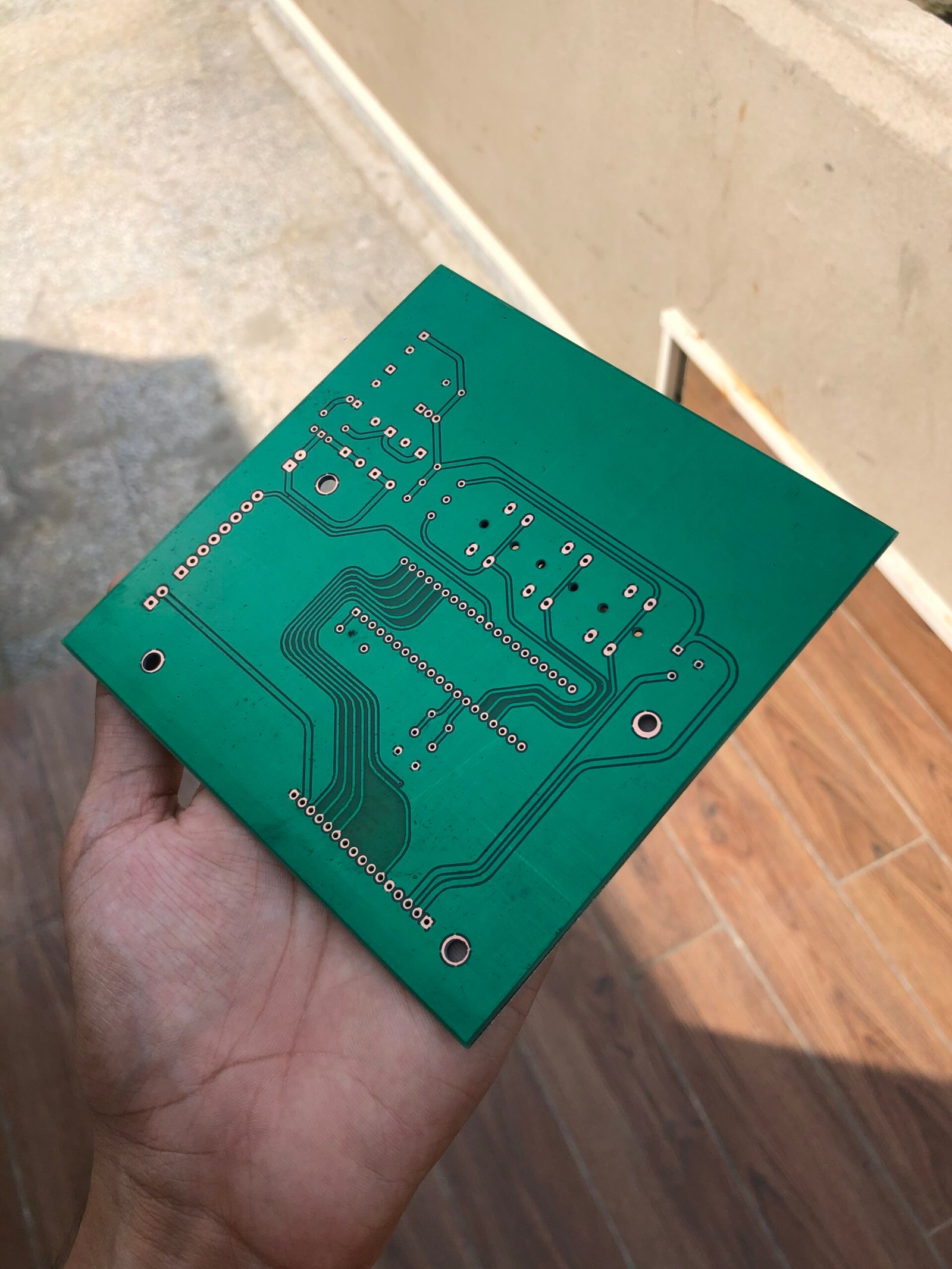
The manufacturing process involves printing a thin layer of copper on the board. Using a method like photolithography, the copper layer is then etched away to form the circuit paths, leaving the conductive traces intact.
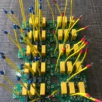
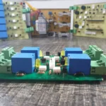
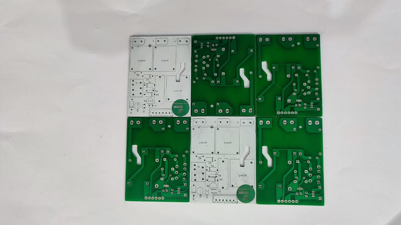
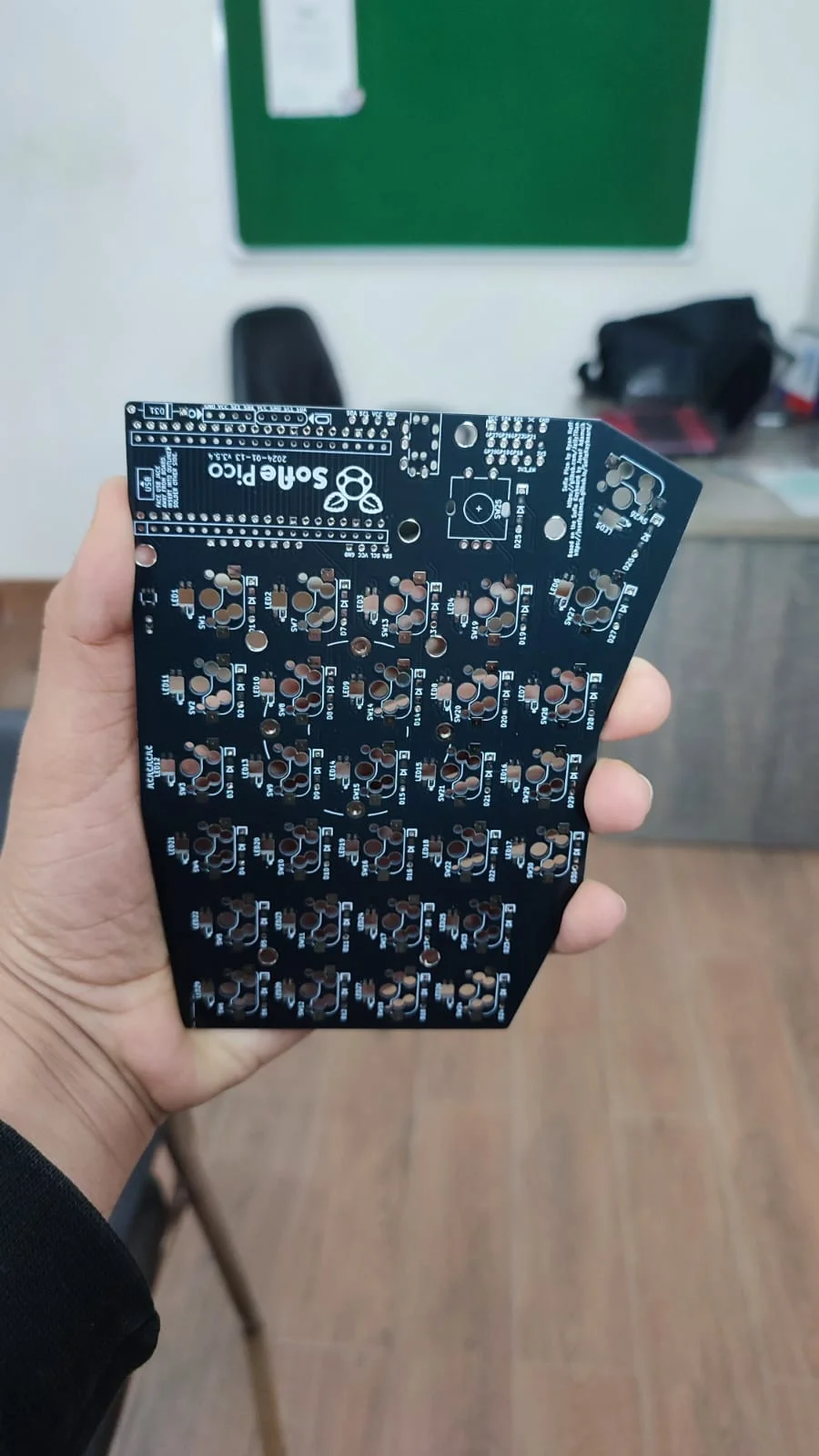
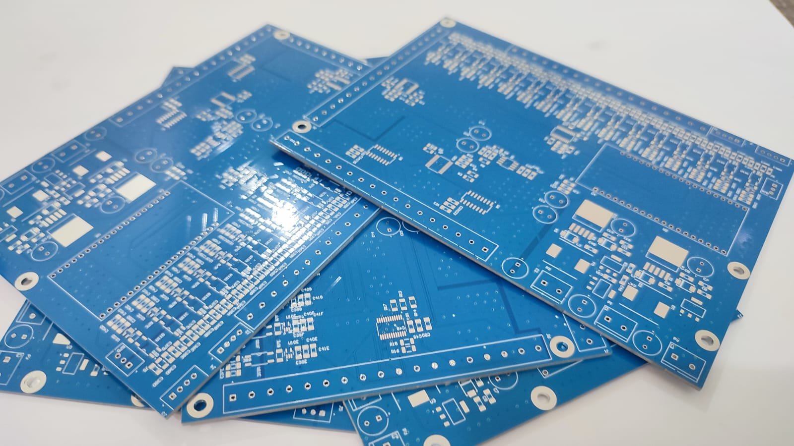
Assembly
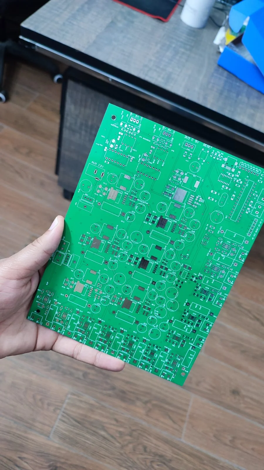
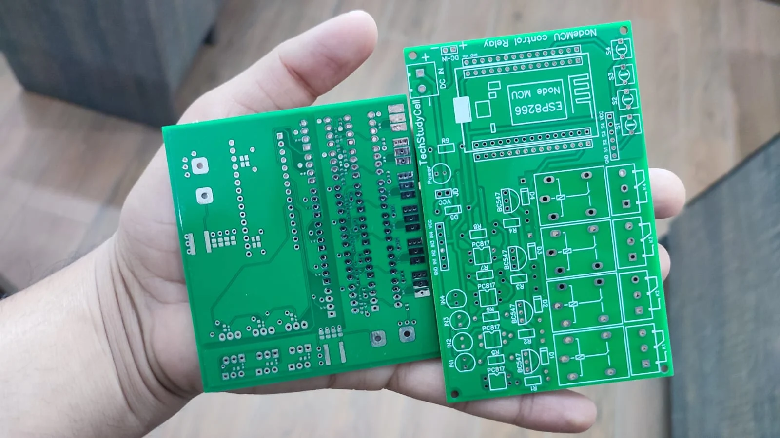
Once the circuit paths are formed, components are placed on the board. This may involve through-hole technology (THT) or surface-mount technology (SMT), depending on the design and application.
Testing and Quality Control
To ensure the PCB performs correctly, it undergoes rigorous testing. This may include visual inspections, electrical testing, and stress testing to simulate real-world usage. Any defective boards are discarded or reworked.
High Precision and Reliability: Modern PCB manufacturing techniques ensure accurate designs and robust connections, leading to better product performance and longevity.
Cost-Effective Production: With automated processes, manufacturers can produce PCBs in bulk at lower costs, making them affordable for a wide range of industries.
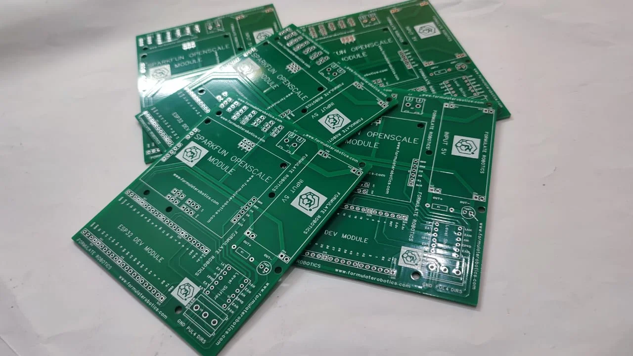
Customization: Depending on the application, PCBs can be customized for size, shape, complexity, and functionality, making them ideal for everything from consumer electronics to industrial machinery.
PCBs are found in virtually every electronic device. Some key applications include:
Consumer Electronics: Smartphones, laptops, and gaming consoles rely on high-performance PCBs to function seamlessly.
Automotive Industry: PCBs are used in various automotive applications, including control systems, navigation, and safety mechanisms.
Medical Devices: Life-saving medical equipment like pacemakers and diagnostic machines depend on reliable PCBs to ensure patient safety.
Industrial Machinery: Automation systems, robotics, and machinery rely on PCBs for efficient operation and control.
A PCB (Printed Circuit Board) is a board used to connect and support electronic components. It is essential for the operation of most electronic devices, providing both structure and electrical pathways.
The most common material is FR4 (a fiberglass-reinforced epoxy laminate). Others include aluminum, polyimide (for flexible PCBs), and ceramic for high-frequency applications.
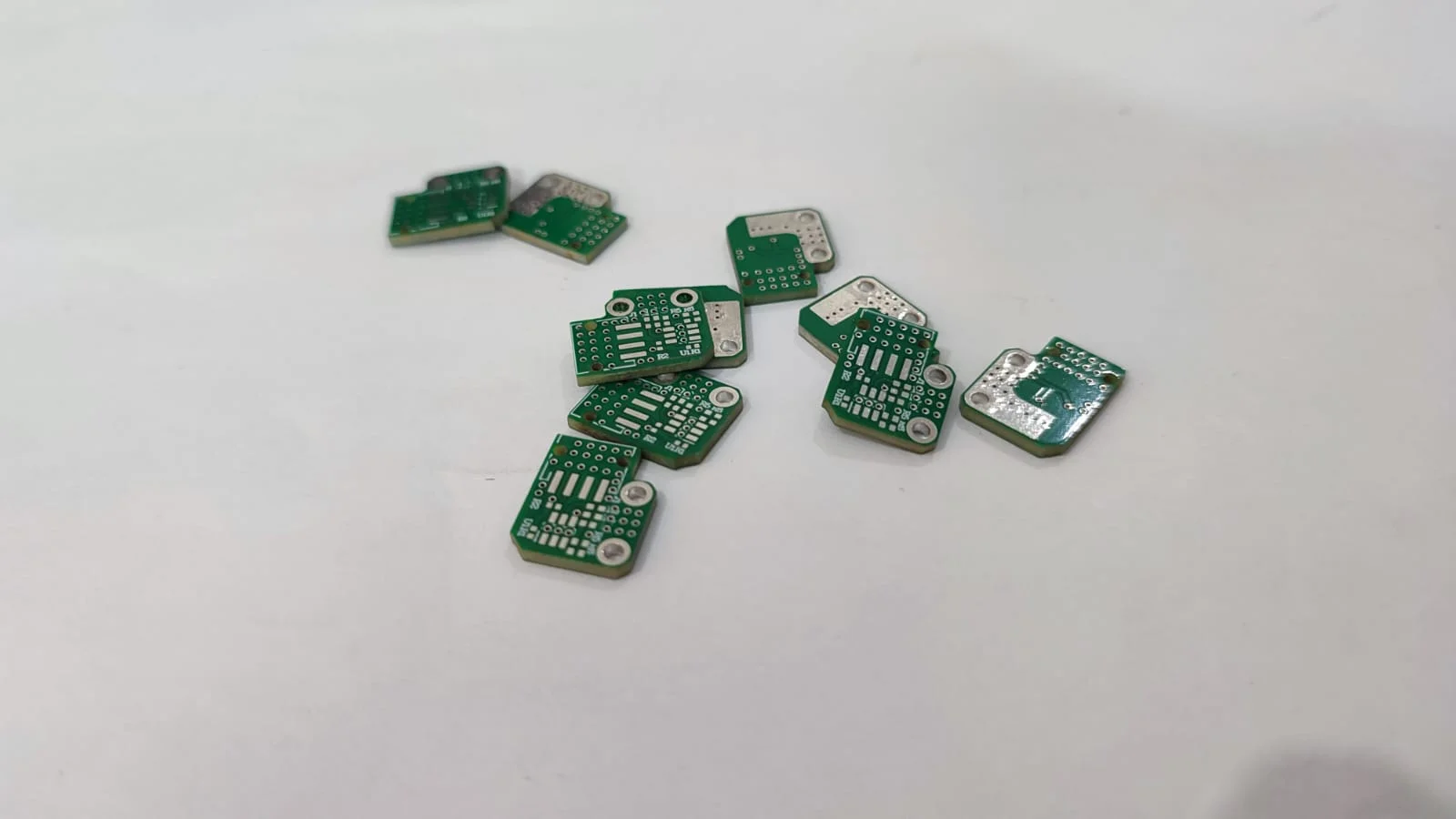
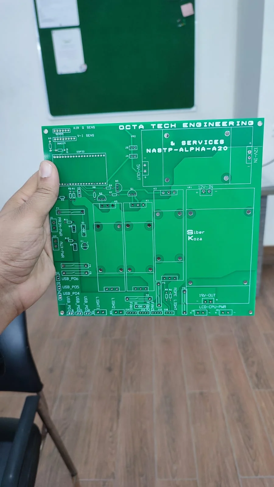
There are several types, including single-sided, double-sided, multi-layer, rigid, flexible, and rigid-flex PCBs, each suited for different applications.
Standard PCB manufacturing can take anywhere from 2 to 10 business days, depending on the complexity, order size, and additional requirements like testing or assembly.
Yes, many manufacturers offer custom PCB fabrication based on your specific design files and requirements, including size, layers, materials, and finishes.
Minimum order quantities vary by manufacturer, but many now offer low-volume or even prototype production starting from as little as 1-5 pieces.
Yes, many PCB manufacturers also provide assembly services, where components are soldered onto the board using SMT or THT techniques.
PCBs are tested using techniques like electrical testing (flying probe or bed of nails), AOI (automated optical inspection), and X-ray to ensure performance and reliability.
Gerber files are the industry standard for PCB manufacturing. Some manufacturers may also accept ODB++, Eagle, or KiCAD files depending on their systems.

If you have any questions about PCB manufacturing or would like to learn more about our fabrication services, feel free to contact our team. Our experts are ready to assist you with tailored solutions and guide you through every stage of your PCB project.

